Reference Electronics · Volume 5
Output Stages — Solenoid and Rumble Drivers, Clamps and LEDs
Why the usual MOSFET is out of its datasheet at 3.3 V, a regulated-current stage for the carrier, where the TVS goes, why two stages never fire together, and the small parts that keep a solenoid from firing on its own
5.1 What the Firmware Asks of the Outputs
OpenFIRE treats the two force-feedback outputs differently (OpenFIREFeedback.cpp, v6.2):
- Solenoid (GP16 by default) is switched with
digitalWrite(HIGH)anddigitalWrite(LOW). There is no PWM. The defaults inOpenFIREprefs.hare 45 ms on, 80 ms off between autofire shots, and a 500 ms hold before single shots repeat. With a TMP36 fitted, a reading above the warning threshold (38 °C) doubles the off time and one above the shutdown threshold (45 °C) stops the solenoid. - Rumble (GP17) is started with
analogWrite(pin, rumbleStrength), default strength 255, and stopped withdigitalWrite(LOW)after the rumble length (default 150 ms). On the Arduino-Pico coreanalogWriteis a PWM at a default 1 kHz.
So the solenoid stage switches tens-of-milliseconds pulses at a few hertz, where switching losses are irrelevant and conduction loss, clamping and boot behaviour are everything. The rumble stage switches a small motor at 1 kHz, where none of it is demanding.
How hard the solenoid hits, how long a pulse it wants and how hot it gets belong to the Solenoid Recoil dive. This volume takes a solenoid as a given inductive load of a few amps and switches it.
5.2 The Community Solenoid Stage
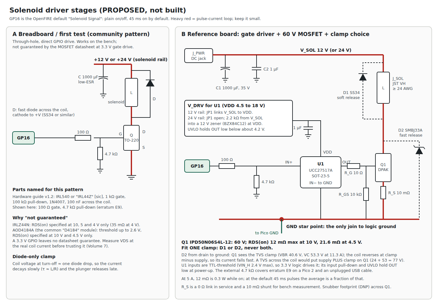
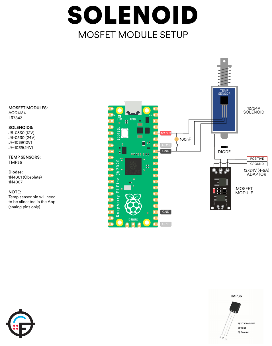
The OpenFIRE hardware guide (version 1.2) draws the solenoid stage as GP16 through a 1 kΩ resistor to the gate of a TO-220 MOSFET, a 100 kΩ resistor from gate to ground, the solenoid from the supply to the drain, a 1N4007 across the coil (“1N4001 (Obsolete)” is listed beside it) and a 100 nF capacitor across the coil, fed from a “12/24V (4-5A) ADAPTOR”. It names the MOSFETs “IRL540” and “IRL44Z”, the second presumably the IRLZ44. An alternative sheet replaces the discrete stage with a MOSFET module and names “AOD4184” and “LR7843” modules.
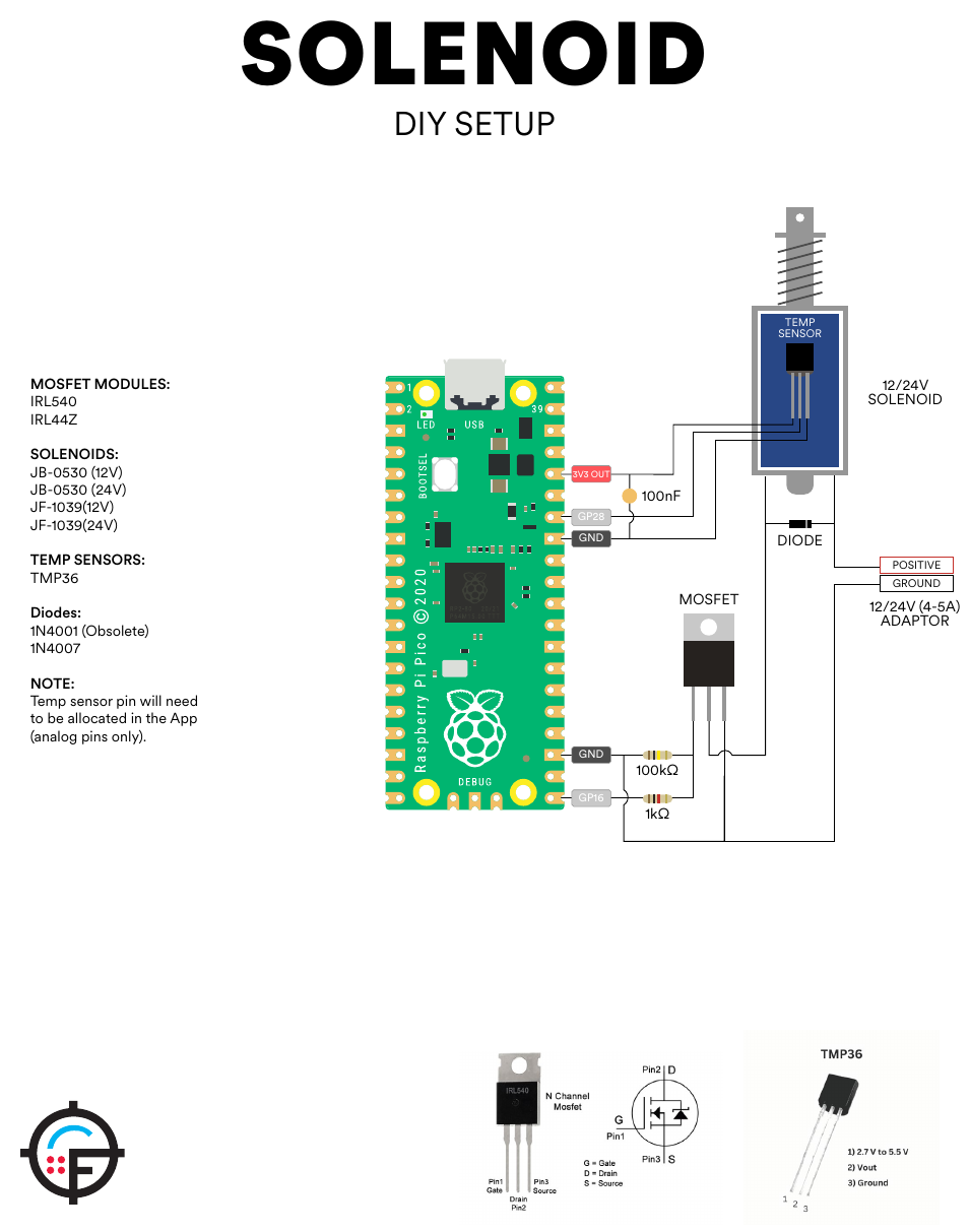
The PICON-AS reference build uses a ready-made “20A Mini 5–26V PWM MOSFET driver board”, an FR207 fast-recovery diode, a 1000 µF 25 V low-ESR polymer capacitor and an optional P6KE16A TVS. Its solenoid, a JF-1039B labelled 400 mA, was measured by its author at about 2 A.
This pattern works, and thousands of guns run on it. It has three weaknesses that a designed board can remove.
5.3 The MOSFET Datasheet Problem
A GPIO at 3.3 V gives a MOSFET a gate drive of at most 3.3 V. The question is whether the MOSFET’s datasheet guarantees an on-resistance at that drive. For the parts the community names, it does not.
Table 1 — 5.3 The MOSFET Datasheet Problem
| MOSFET | VDS | Threshold VGS(th) | RDS(on) guaranteed at | Source |
|---|---|---|---|---|
| IRLZ44N (TO-220) | 55 V | 1.0 to 2.0 V | 22 mΩ at 10 V; 25 mΩ at 5 V; 35 mΩ at 4 V | Infineon/IR datasheet |
| AOD4184A (TO-252), the “D4184” module part | 40 V | 1.7 to 2.6 V (2.1 typical) | under 7 mΩ at 10 V; under 9.5 mΩ at 4.5 V | AOS datasheet |
| AO3400A (SOT-23) | 30 V | 0.65 to 1.45 V | under 26.5 mΩ at 10 V; under 32 mΩ at 4.5 V; under 48 mΩ at 2.5 V | AOS datasheet |
| IPD50N06S4L-12 (TO-252) | 60 V | 1.2 to 2.2 V | 12 mΩ max at 10 V; 21.6 mΩ max at 4.5 V | Infineon datasheet |
The AOD4184A is the clearest case. Its threshold can be as high as 2.6 V, which leaves 0.7 V of overdrive from a 3.3 V pin on a worst-case part, and its datasheet says nothing about its resistance below 4.5 V. On a typical part at room temperature it will probably work; on a hot part at the end of a long session, with a GPIO that sags under load, the datasheet offers no assurance. The IRLZ44N is better, with a 2 V maximum threshold, but its lowest specified point is 4 V.
Only the AO3400A in that table is specified below 3.3 V, and at 30 V it is not a part for a 24 V solenoid whose turn-off spike has to be clamped somewhere.
There are two honest ways out:
- Measure it. For a breadboard, use the IRLZ44N, drive it from the GPIO, and measure the drain-source voltage at the real solenoid current. If VDS is a few tenths of a volt at the coil’s peak current, the part is adequately on. That measurement is in Volume 7, and it is the right way to qualify panel A of the figure.
- Give the gate a proper drive. A gate driver powered from the solenoid rail lifts the gate to 12 V, which puts any logic-level or standard MOSFET deep into its guaranteed region.
The discrete stage below takes the second way; the regulated stage of 5.12 does too, with its own internal gate drive.
5.4 The Discrete Stage
Decision D13 (5.12) moved the carrier board to a regulated stage. The discrete switching stage below remains the breadboard stage, the constant-voltage condition the Solenoid Recoil bench sweeps run in, and the reference for a coil above 4.1 A; everything said about it still holds.
The driver: TI UCC27517A. A single-channel low-side driver in SOT-23-5. The datasheet points that make it suitable:
- VDD from 4.5 V to 18 V, so it runs directly from a 12 V solenoid rail.
- TTL-compatible inputs independent of VDD: input high threshold 2.2 V typical, 2.4 V maximum; input low threshold 1.0 V minimum. A 3.3 V GPIO drives it with margin.
- Under-voltage lockout: the supply start threshold is 3.91 / 4.20 / 4.5 V (min / typ / max) at 25 °C and 3.70 to 4.65 V over temperature, and the datasheet states that outputs are “Held Low During VDD UVLO”.
- “internal pull-up and pull-down resistors on the input pins ensure that outputs are held low” when the inputs float.
- ±4 A peak source and sink.
The MOSFET: Infineon IPD50N06S4L-12. A 60 V, AEC-Q101 part in TO-252 with RDS(on) of 12 mΩ maximum at 10 V of gate drive, 33 mJ single-pulse avalanche rating, and 30 nC typical gate charge. At 12 V of drive it is fully enhanced. At a 5 A solenoid current it dissipates 0.3 W while on; at the default 45 ms on in a 125 ms autofire cycle that averages about a tenth of a watt, which a TO-252 on a modest copper pour handles without notice.
Sixty volts is the choice because of the clamp (5.6): it leaves room for a TVS that turns the coil off quickly on either a 12 V or a 24 V rail.
The supply for the driver. The rail is now decided as 24 V class, 18 to 28 V (D14), on which the driver would exceed its 18 V maximum, so VDD is taken from a 12 V zener (BZX84C12) fed through 2.2 kΩ from V_SOL. The wave-2 jumper JP1, which fed a 12 V rail straight to VDD, is no longer needed. That draws about 5.5 mA and dissipates about 66 mW in the resistor. The driver’s own consumption is small and the gate charge per pulse is drawn from a 1 µF capacitor at its VDD pin.
The gate network. A 10 Ω resistor between the driver and the gate (R_G) sets the edge rate; it is the first knob for EMI (5.7). A 10 kΩ resistor from gate to source (R_GS) holds the MOSFET off when the driver is unpowered, for instance with the solenoid adapter plugged in and nothing else.
The current-sense position. The source returns through R_S, the board’s on-board sense position (not the 0.1 Ω bench shunt of the Solenoid Recoil rig, which sits in that rig’s coil return; the regulated stage of 5.12 has no shunt and reads its current from IPROPI), fitted as a 0 Ω link in service and as a 10 mΩ resistor on the bench, so that the solenoid current can be captured as a voltage (50 mV at 5 A) on the Analog Discovery without clamping a probe around a wire.
5.5 Keeping the Solenoid Off When It Should Be Off
Requirement R5 in Volume 1 says the solenoid must never fire at power-up, during a settings save, or with the USB cable unplugged and the solenoid adapter live. Each case is covered by a specific part.
Table 2 — 5.5 Keeping the Solenoid Off When It Should Be Off
| Case | What happens without design | What prevents it |
|---|---|---|
| Power-up, before firmware runs | RP2040 pads come out of reset with their pull-down enabled (PDE = 1 in the datasheet’s pad register reset values), 50 to 80 kΩ | the internal pull-down, plus the 4.7 kΩ external pull-down at the driver input |
| Settings save from the app | firmware sets GP16 to an input while it restarts the camera (Volume 2) | the 4.7 kΩ pull-down; on an A2-stepping Pico 2 a 100 kΩ pull-down would not hold the pad below about 2.2 V (erratum RP2350-E9) |
| USB unplugged, solenoid adapter live | the Pico is unpowered; GP16 floats | the 4.7 kΩ pull-down and the driver’s internal input pull-down; R_GS on the MOSFET gate |
| Driver unpowered (24 V rail, zener not yet up) | driver output undefined | UCC27517A holds its output low in UVLO; R_GS holds the gate |
| Regulated stage (5.12), any of the above | DRV8251A input floating or low | 4.7 kΩ external plus the driver’s 100 kΩ internal pull-down; both inputs low means coast, then sleep; VREF comes from 3V3, so with the Pico unpowered the trip current is zero |
| Port stage while the recoil fires (D16) | firmware error raises EJECT_CMD | Q4 holds the port stage’s input low while SOL_CMD is high (5.13) |
| Fast drain voltage step when the adapter is plugged in | the drain-gate capacitance couples the step into a floating gate | R_GS, and the driver’s low output impedance when powered |
Panel A of the figure carries the same 4.7 kΩ in place of the guide’s 100 kΩ, for the same reasons. It costs 0.7 mA from the GPIO while the solenoid is on.
5.6 The Clamp: Diode or TVS, and Where
This section is about the discrete stage of 5.4. The regulated stage of 5.12 needs no coil clamp: at the end of a shot its bridge coasts, and the coil’s current returns to the supply through the driver’s body diodes.
When the MOSFET turns off, the coil’s current has to go somewhere. Where it goes sets how fast the solenoid releases, which matters for how crisp a kick feels and how fast autofire can run. The physics belongs to the Solenoid Recoil dive; the circuit choice belongs here.
A diode across the coil (D1, “soft release”). The coil current circulates through the diode. The voltage across the coil during that time is one diode drop, so the current decays slowly, with a time constant of roughly L/R, and the MOSFET never sees more than the supply plus a diode drop. It is the safest arrangement and the slowest release. A Schottky or fast-recovery diode is preferred to a 1N4007; the reference board uses an SS34 (40 V, 3 A), which covers a 24 V rail.
A TVS from drain to ground (D2, “fast release”). With no diode across the coil, the drain flies up until the TVS conducts. The coil then sees the clamp voltage minus the supply in reverse, which collapses its current far faster. The reference part is a Littelfuse SMBJ33A: 33 V stand-off, 40.6 V breakdown, 53.3 V clamping at 11.3 A, 600 W for a 10/1000 µs pulse. With the TVS from drain to ground, the MOSFET sees at most the clamp voltage, about 53 V, which a 60 V part tolerates.
The mistake to avoid: a TVS across the coil. The PICON-AS list’s optional P6KE16A and many forum circuits put a TVS or Zener across the coil instead. That works too, but then the MOSFET sees the supply plus the clamp. With an SMBJ33A across a coil on a 24 V rail, that is 24 + 53 = 77 V, over a 60 V MOSFET’s rating. A TVS across the coil must be chosen together with the supply voltage and the MOSFET; a TVS from drain to ground is independent of the supply.
Never fit both. With D1 fitted, the drain never rises high enough for D2 to conduct, so the board offers both footprints and the build fits one.
The energy check. Whatever the TVS absorbs on each shot is roughly the energy stored in the coil, ½ L I², plus what the supply delivers during the clamp. The solenoid’s inductance is not published for the parts named in the community lists. It is a bench measurement (Volume 7) and then a check against the TVS’s pulse rating. For small solenoids at a few amps the 600 W rating of an SMB part is expected to be ample, but that is to be confirmed, not assumed.
The 100 nF capacitor that the hardware guide places across the coil slows the edge and absorbs some of the ringing; on the reference board a snubber footprint across the MOSFET does the same job with values chosen on the bench.
5.7 Local Energy and the Current Loop
Bulk capacitance at the board. A solenoid pulse is a few amps for tens of milliseconds, drawn through an adapter and a cable. The PICON-AS build fits a 1000 µF low-ESR polymer capacitor; the reference board does the same at the input connector (C1, 35 V rating so that one part serves both rails) with a 1 µF ceramic (C2) close to the coil, diode and MOSFET. Sizing a pulse bank for a battery build is the Power Supplies dive’s subject. With the regulated stage, C1 also absorbs the energy each coil returns at the end of a shot, about 2.5 V of rise (5.12).
The loop. The heavy red path in the figure (C1 or C2, the coil connector, the MOSFET, the shunt and back to C1) carries the pulse current. Its area is what radiates. On the PCB it is kept as small as the parts allow and runs over its own ground copper, which joins the logic ground at one point (Volume 8).
Wire gauge. OpenFIRE’s README puts it bluntly: “Solenoid may cause EMI disconnects with too thin of wiring. Cables for this run specifically should be 24AWG at its thinnest - or else the cables will become antennas under extended use, which will trip USB safety thresholds in your PC to protect the ports.” The ESP32 port’s README repeats the 24 AWG figure. Gauge is not really the EMI mechanism; loop area and edge rate are. But the observation is real, and thicker leads twisted as a pair from board to coil address both resistance and loop area. The reference harness uses 22 AWG twisted pair for the coil.
5.8 The Rumble Stage
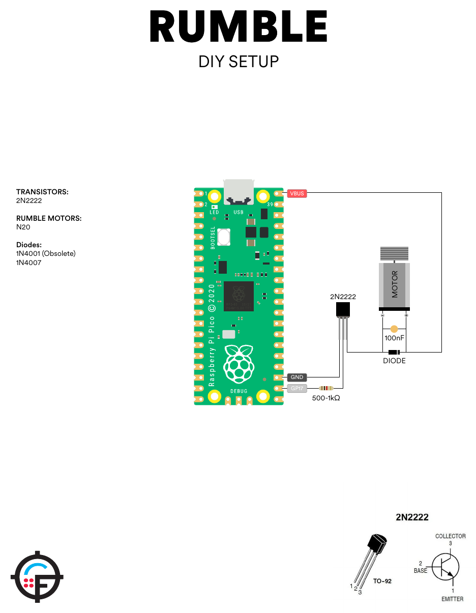
The hardware guide drives the rumble motor with a 2N2222 transistor from GP17 through 500 Ω to 1 kΩ, with the motor on VBUS and a 1N4007 and 100 nF across it, and names an “N20” motor. The reference board replaces the bipolar transistor with an AO3400A, which the AOS datasheet specifies at under 48 mΩ with only 2.5 V of gate drive, so a 3.3 V GPIO is fully inside its guarantees. A 100 Ω gate resistor, a 4.7 kΩ pull-down (same reasons as 5.5), an SS34 across the motor, 100 nF across the motor terminals and a 100 µF capacitor on VBUS complete it.
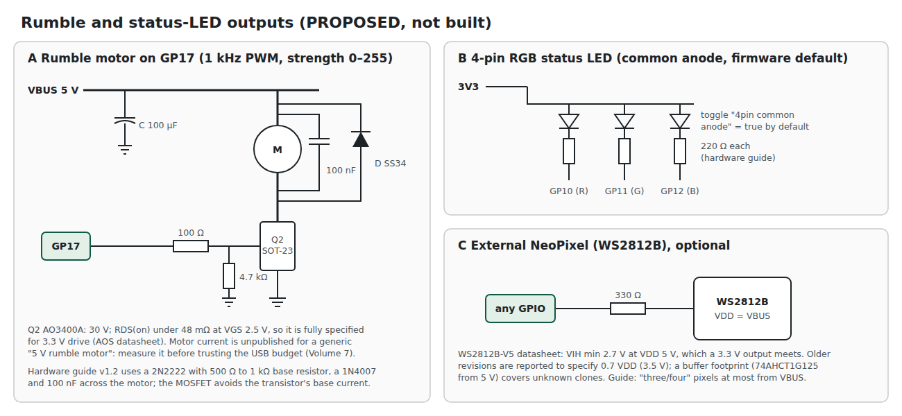
The motor’s current is the open number. A “5 V rumble motor” is not a specification. Because the motor runs from USB VBUS, its current, inrush included, decides whether a wired gun stays inside a USB port’s budget. It is the first measurement in Volume 7.
5.9 Status LEDs and NeoPixels
The pick for the first gun is one NeoPixel on GP10, because Volume 2’s pin budget needs GP11 and GP12 for other things; the RGB option below remains if the pins are free.
RGB LED. The firmware supports a four-pin RGB LED on GP10, GP11 and GP12, with a toggle, “4pin common anode”, that defaults to true. The hardware guide wires it with 220 Ω per colour, either to 3V3 (common anode) or ground (common cathode). At 3.3 V and a red LED’s forward voltage of about 2 V, that is a few milliamps per pin.
NeoPixels. The firmware drives WS2812B pixels from any GPIO. The hardware guide powers them from VBUS and says “Up to three/four NeoPixels can be run directly off VBUS - any additional pixels should be driven by external voltage due to USB amp draw limitations.” The data line is 3.3 V into a part powered at 5 V. The WS2812B-V5 datasheet gives the high-level input as 2.7 V minimum at VDD 5 V, which a 3.3 V output meets. Older datasheet revisions are reported to specify 0.7 × VDD, which at 5 V would be 3.5 V and out of reach; that older figure was not confirmed from a primary source here. Since clone pixels are common and their datasheets rarely known, the reference board carries a footprint for a 5 V buffer with TTL-level inputs (SN74AHCT1G125) that can be fitted or bridged.
5.10 Ready-Made MOSFET Modules
The small red or green “MOSFET trigger switch” modules sold for Arduino projects, typically with two paralleled D4184 parts, are what most builders use, and the hardware guide’s alternative sheet shows one. They are fine for a first gun with three caveats from this volume: the gate is driven at 3.3 V outside the AOD4184A’s guarantees (5.3); the gate pull-down on such modules is whatever its maker fitted, which matters for 5.5; and the clamp arrangement is whatever is on the module, often a diode across the output terminals. For a designed board, the stage in 5.4 replaces the module outright.
5.11 A Second Power Output for the Ejection Port
Decision (D5, 2026-10-18): try both ways of moving the MP7’s ejection port: one solenoid that gives the kick and moves the port, and a separate actuator for the port. The first needs nothing from this board beyond the solenoid stage. The second needs a second power output, and the board has to provide it from the first spin or the comparison cannot be made.
What the firmware offers. Nothing, directly. OpenFIRE’s pin functions include exactly two force-feedback outputs, “Solenoid Signal” and “Rumble Signal” (boardInputs_Strings, v6.2); there is no third. Wave 2 offered two ways to command a port actuator, in parallel with the solenoid on SOL_CMD or on its own pin. Decision D16 (5.13) rules out the first, because it fires both coils at once. That leaves one:
- On its own pin, from the fork. EJECT_CMD on GP11 (Volume 2’s pin budget), driven by the fork with whatever timing the port wants: every shot, only on the last round, or held open on a reload. This is a firmware change under decision D10 and belongs to the Our Firmware dive.
The stage. The carrier board carries a second copy of the regulated stage of 5.12, U5, a DRV8251A with its own 4.7 kΩ input pull-down, current-set divider, R_IPROPI and a second JST VH connector, with its input on EJECT_CMD through the interlock of 5.13. Fitting a second identical stage, rather than a smaller one, is deliberate: the actuator has not been chosen (Moving Ejection Port owns it), and a stage that can drive the main solenoid can drive anything smaller. Every R5 case in 5.5 applies to it unchanged.
What it does to the supply. Because the two stages never fire together (D16, 5.13), the peak current on the solenoid rail is one stage’s trip current, not the sum. The two stages share the bulk capacitor and the single ground join; their pulse loops are laid out side by side, not nested (Volume 8).
If the actuator turns out to be a hobby servo, the power stage is not used: a servo wants a 5 or 6 V supply and a pulse-width signal, which GP11 can produce from the fork. The stage’s footprints stay empty and nothing else changes.
Its temperature. A second actuator that runs every shot gets as hot as the main solenoid. The pin budget reserves GP27 (ADC1) for a second TMP36, read by the fork; stock OpenFIRE reads only one.
5.12 The Regulated Stage (Decision D13)
Decision (D13, 2026-10-18): regulated current from the first driver board. The reason is the one the Solenoid Recoil dive gives: a stage that sets the current sets the ampere-turns and so the force, and the coil’s resistance, its temperature, the wiring and the supply drop out of the kick. That dive’s model puts the spread across six coils at 2.6 to 1 on a fixed voltage and about 1.1 to 1 under regulation. Decision D14 fixes the rail the stage works from: 24 V class, 18 to 28 V working, with coils of the “6 to 12 V” class, roughly 5 to 12 Ω, run at 1 to 2.5 A, so that the hot coil’s I·R is about half the rail (Solenoid Recoil Vol 8, rows SR-1 to SR-3).
That dive specifies what the stage must do:
- Hold a set current, settable per gun, from a rail with a forcing ratio near two.
- Chop with slow decay while holding, so the ripple stays small and little energy is lost per cycle.
- Decay fast at the end of the shot, so the plunger is released promptly.
- End the pulse at landing, which is the firmware’s job and unchanged by the stage.
To those this board adds its own: it must be safe in every case of requirement R5 (5.5), work with the stock firmware’s plain on/off solenoid output (5.1), stay inside the 60 V parts and margins the rest of the design uses, and be buildable in the lab.
5.12.1 The four ways to regulate it
Table 3 — The four ways to regulate it
| Approach | How it works | For | Against |
|---|---|---|---|
| A. Hysteretic chopper, discrete | the low-side MOSFET of 5.4 with a sense resistor; a comparator with hysteresis turns the gate off at the upper current and on at the lower; the coil freewheels through a diode while off | any current, any switch; the chop frequency is chosen by the hysteresis band | a comparator, a reference, a sense resistor and its loss, and a second switch in the freewheel path if the end of the shot is to decay fast (a diode alone gives the slow L/R release; a Zener in the path burns energy on every chop cycle) |
| B. Dedicated solenoid controller (TI DRV110) | peak and hold: a fast ramp to a peak current, held for a capacitor-set time, then a lower hold current, chopped at about 20 kHz through an external MOSFET and sense resistor | made for solenoids; one chip; a quiet chop frequency | the profile is a valve’s (peak, then hold), not a kick’s; release through the freewheel diode is slow; and its datasheet says “The EN pin contains an internal resistor network to set the pin to logic HIGH when the EN pin is floating”, so an unpowered Pico with the brick live would fire the coil unless EN is held low by an external part |
| C. Buck-type constant-current stage | a constant-current buck converter (the LED-driver kind) with the coil as its load | very good current accuracy at steady state | the coil is already an inductor, so the buck’s own inductor is a second one in series that slows the rise the kick depends on; such controllers soft-start; and there is no fast-decay path at the end |
| D. MCU closed loop | the microcontroller samples a shunt on its ADC and adjusts a PWM duty to hold the current | no extra silicon | no ADC pin is free (Volume 2); the RP2040’s ADC is shared with the Hall trigger; a firmware fault or a hang leaves the current uncontrolled, the failure mode regulation exists to prevent; and the stock firmware cannot do it |
| E. H-bridge driver with integrated current regulation (TI DRV8251A) | an N-channel H-bridge with a current mirror; above a set trip current it brakes (both low-side switches on, slow decay) for a fixed 25 µs, then drives again; with both inputs low it coasts, and the coil current returns to the supply through the body diodes | one chip per stage, no power shunt; slow decay while holding and fast decay at the end, both built in; works from a plain on/off input; 48 V rated | 4.1 A peak; chop frequency set by the coil and the rail, not chosen; the returned energy goes into the bulk capacitor |
The usual four classes are A to D; the fifth, E, is the one that meets every requirement at once. A motor driver is a fair tool here because a solenoid is the “other resistive and inductive load” such parts are sold for, and the bridge gives the fast decay that a single low-side switch cannot.
5.12.2 The pick: TI DRV8251A, one per stage
From Texas Instruments’ datasheet (SLVSFU6, January 2022):
Table 4 — From Texas Instruments' datasheet (SLVSFU6, January 2022)
| Parameter | Value | Why it matters here |
|---|---|---|
| Supply | 4.5 to 48 V operating; 50 V absolute maximum | the 18 to 28 V rail and the 24 V brick’s upper over-voltage band (32.4 V, Power Supplies PS-6) sit well inside |
| Output | 4.1 A peak (overcurrent trip 4.1 A minimum above 5.5 V) | covers the 1 to 2.5 A of SR-3 with margin |
| On-resistance | 225 mΩ high side + 225 mΩ low side, typical, at 24 V | 2.8 W while driving 2.5 A; about 0.45 W averaged over a 20 ms shot in a 125 ms autofire cycle, 18 °C over ambient at the datasheet’s 40.4 °C/W |
| Current sense | current mirror on IPROPI, 1575 µA/A typical, ±5 % | the set point and a bench current signal without a power shunt |
| Regulation | trip at ITRIP; then brake (low-side slow decay) for tOFF = 25 µs; blanking 1.4 µs | slow decay while holding (requirement 2) |
| Off state | IN1 = IN2 = 0: “Coast; H-bridge disabled to High-Z (sleep entered after 1 ms)“ | fast decay at the end (requirement 3): the coil drives its current back into V_SOL through the body diodes, at about −(V_SOL + 1.6 V) |
| Inputs | VIH 1.5 V minimum, 100 kΩ internal pull-down on each input | a 3.3 V GPIO drives it; a floating input is off |
| Wake | up to 250 µs from an input edge out of sleep | a fraction of a millisecond added to a 10 to 45 ms shot; nothing to the feel |
| Package | HSOP-8 with exposed pad, 4.9 × 6.0 mm | reflowed in the lab; the pad is the heat path |
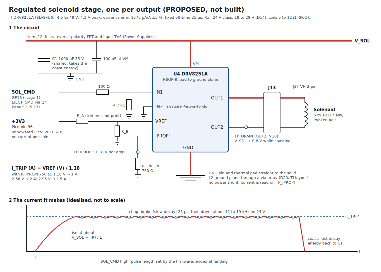
Setting the current. The trip current follows the datasheet’s equation 3, ITRIP × AIPROPI = VREF / RIPROPI. With R_IPROPI = 750 Ω, ITRIP in amps is VREF in volts divided by 1.18: 1.18 V for 1 A, 2.36 V for 2 A, 2.95 V for 2.5 A, which keeps IPROPI under the 3.0 V at which the ±5 % accuracy is specified. VREF comes from a divider on the Pico’s 3V3 with a footprint for a trimmer, so the set point is a resistor choice per gun, made on the bench against the measured kick (Volume 7). Two properties follow from taking VREF from 3V3: with the Pico unpowered, VREF is zero and the stage cannot drive any current at all, which is one more layer under R5; and the set point moves with the Pico’s 3V3 regulator, a fraction of a percent, well inside the mirror’s ±5 %. A firmware-set current (a filtered PWM on VREF) needs a pin the budget does not have; it is a Stage 2 option.
The chop frequency is an estimate, not a choice. With a fixed off time, the stage drives for as long as it takes to recover what the coil lost during 25 µs of braking. During the brake the coil sees roughly its own I·R; while driving, the rail minus I·R. So the on time is about tOFF × (I·R) / (V_SOL − I·R), independent of the inductance. At 2 A in a hot 8 Ω coil on 24 V (forcing ratio 1.5) that is about 58 µs on and 25 µs off, about 12 kHz; at a forcing ratio of 2 it is about 28 µs on, about 19 kHz. The ripple, V × tOFF / L, is 0.06 A or less with the inductances in the Solenoid Recoil model. Twelve to nineteen kilohertz is at the top of the audible range, so the coil may sing faintly under the impact. Whether that is heard is a bench question (Volume 7); the solenoid’s own clack is far louder. These figures are arithmetic from the datasheet and the sibling dive’s model, with the plunger’s back-EMF ignored.
Where the energy goes at the end. In coast, the coil’s stored energy returns to V_SOL. The Solenoid Recoil model puts it at about 0.06 J with the plunger seated; into the board’s 1000 µF that lifts the rail by about 2.5 V. A wall brick cannot sink current, so the bulk capacitor has to take it, and its voltage rating (35 V, Power Supplies PS-6) still covers the GST brick’s over-voltage band plus that rise. Nothing is burned in a clamp, which is why the coil-clamp footprints of 5.6 are not needed on the regulated stage.
What it does to the input protection. The DRV8251A’s 50 V absolute maximum is above the rail and every brick band, but not above the SMBJ33A’s full clamping voltage (53.3 V at 11.3 A), the input TVS first proposed. The input TVS is therefore the SMBJ28A (decision D33, 19 October 2026), which clamps at about 45 V at its rated current, and its 28 V stand-off is the top of the working window. The input TVS belongs to the Power Supplies dive (PS-7). The datasheet also limits how fast VM may rise, 2 V/µs, which matters when power arrives on a plug being pushed home: the bulk capacitor and the cable’s inductance set that slope, and it is measured in Volume 7. With the GX connector at the base plate (D31) the plug is always mated before the brick goes into the wall, so the rail rises on the brick’s own start-up instead.
The current signal for the bench. IPROPI reads the current while driving and while braking, but “In coast mode, the current is freewheeling and cannot be sensed”. The coast is still visible: while the coil is returning its energy, OUT2 sits at about V_SOL + 0.8 V, and it drops when the current reaches zero, so the decay time is read off the output voltage (Volume 7). The regulated stage therefore has no power shunt at all. A 10 mΩ sense resistor in the driver’s ground return, as the discrete stage has, would have to sit between the driver’s thermal pad and the ground plane, and TI’s datasheet asks for the opposite: “Connect to board ground. For good thermal dissipation, use large ground planes on multiple layers, and multiple nearby vias connecting those planes.”
Why not the others.
- DRV8874 (the same family’s 6 A part, 37 V operating, 40 V absolute maximum) was the first candidate. Its 40 V limit sits only 7.6 V above the GST brick’s upper over-voltage band and inside the input TVS’s breakdown range. It also has an nSLEEP pin and a cycle-by-cycle mode that would allow a firmware-set chop frequency, which is its one advantage.
- The discrete chopper (A) would do the job with the 60 V parts of 5.4 and a chop frequency chosen to be inaudible, at the cost of a comparator, a reference, a sense resistor dissipating at the full current, and a second switch for the fast release. It is the path if the bench shows the DRV8251A singing, or if a coil needs more than 4.1 A.
- The DRV110 (B) fails R5 unless EN is held low externally, and its peak-then-hold profile and slow release are the wrong shape for a kick. It remains the right part for a port that must be held open (Moving Ejection Port).
- A buck constant-current stage (C) adds an inductor to a load that is already one.
- MCU closed loop (D) has no pin, and makes the firmware the only thing between a fault and an uncontrolled coil.
What stays from 5.4. The UCC27517A and IPD50N06S4L-12 stage is not on the carrier any more. It remains the breadboard stage for the Solenoid Recoil bench, where the sweeps run in constant-voltage mode until this board exists, and the reference if a coil ever needs more than the DRV8251A’s 4.1 A. With the rail now decided as 24 V class (D14), its gate driver is fed from the 12 V Zener; the JP1 option for a 12 V rail is no longer needed.
5.13 Never Both at Once (Decision D16)
Decision (D16, 2026-10-18): the recoil stage and the ejection-port stage never fire at the same instant; they are sequenced. The supply is sized for one stage (a GST60A24-class brick, Power Supplies), which removes the larger-brick and 50 V-capacitor case. The firmware has to interlock the two outputs, and the board backs it up.
What changes from wave 2. The jumper that let the second stage take SOL_CMD, so that the port moved on the solenoid’s timing with stock firmware, is removed: that arrangement is exactly the simultaneous firing D16 rules out. The second stage now takes EJECT_CMD only (GP11, from the fork). Decision D5’s first option, one solenoid that gives the kick and moves the port, uses the recoil stage alone and needs nothing from the second.
The firmware interlock (the fork, D10). The fork schedules the port pulse after the recoil pulse has ended and its current has decayed, never during it. With the coast release the decay is short: a 2 A current in a seated coil of the model’s 44 mH, driven down by about 25 V, is gone in roughly 3.5 ms. The rule for the Our Firmware dive: EJECT_CMD may rise only when SOL_CMD has been low for at least the measured decay time (Volume 7), and SOL_CMD wins any conflict.
The hardware interlock. One small N-channel MOSFET, Q4 (an AO3400A, the rumble stage’s part, specified at 2.5 V of gate drive), with its gate on SOL_CMD and its drain on the second stage’s input, after a 1 kΩ series resistor from GP11. While SOL_CMD is high, the port stage’s input is held low whatever the firmware does. It costs two parts and gives the recoil stage priority in hardware. The reverse, blocking the recoil while the port fires, is left to firmware: the kick is the function that must never be lost, and the port stage’s coast returns current to the rail rather than drawing it, so a late overlap at the port’s tail does not add to the brick’s load.
What it does to the supply. The peak on V_SOL is one stage’s trip current, not the sum. The fuse, the brick and the bulk capacitor are sized for one stage (Power Supplies Vol 2).
5.14 Why This, and Why Not the Others
Every part this volume picks, with the alternatives it beat. The criteria for the carrier’s solenoid stage were: regulated current with slow decay while holding and fast decay at the end (D13); a supply rating with margin over the 18 to 28 V rail and the brick’s over-voltage band (D14); defined behaviour in every R5 case; and parts the lab can solder. The discrete stage was judged on guaranteed on-resistance at the gate drive actually available and a drain rating above the worst clamp voltage on a 24 V rail.
Table 5 — 5.14 Why This, and Why Not the Others
| Function | Pick | Alternatives | Why the pick, and why not the others |
|---|---|---|---|
| Carrier solenoid stage (D13) | TI DRV8251A per stage, fixed off-time regulation, VREF divider, R_IPROPI 750 Ω | DRV8874; discrete hysteretic chopper; DRV110 peak and hold; buck constant-current; MCU closed loop; plain low-side switch (wave 2) | One chip gives the set current, slow decay while holding and fast decay at the end, from a plain on/off input, rated 48 V. DRV8874: 40 V absolute maximum, too close to the brick and TVS bands. Discrete chopper: more parts and a sense resistor at full current; kept as the fallback if the DRV8251A sings or a coil needs over 4.1 A. DRV110: EN floats high (fails R5), valve-shaped profile, slow release. Buck: a second inductor in series with the coil. MCU loop: no pin, and the firmware becomes the only safeguard. Plain switch: does not regulate (D13). |
| Port-stage interlock (D16) | AO3400A (Q4) holding the port input low while SOL_CMD is high, plus the fork’s sequencing | firmware only; a logic gate | Two parts, recoil priority in hardware. Firmware alone leaves a bug able to fire both. A gate adds a supply-powered part and a package for the same function. |
| Gate drive (discrete stage) | TI UCC27517A from the solenoid rail | GPIO straight to a logic-level MOSFET; a ready-made MOSFET module; a discrete transistor level shifter | The pick gives 12 V of gate drive from a 3.3 V input with TTL thresholds (2.4 V max high), holds its output low in UVLO and has input pull-downs. Direct drive leaves the IRLZ44N and AOD4184A outside their datasheets (5.3). Modules bring an unknown pull-down and clamp (5.10). A discrete level shifter costs more parts and has no undervoltage lockout. |
| Solenoid MOSFET (discrete stage) | Infineon IPD50N06S4L-12 | AOD4184A; IRLZ44N; AO3400A | 60 V covers the drain-to-ground TVS’s 53.3 V clamp on a 24 V rail, with 12 mΩ max at 10 V. The AOD4184A is 40 V, below that clamp. The IRLZ44N’s 55 V leaves under 2 V of margin over the clamp and is through-hole. The AO3400A is 30 V. |
| Clamp, soft release (discrete stage) | Slkor SS34 Schottky (40 V, 3 A) across the coil | 1N4007; FR207 | Fast and low-drop; the 1N4007 the guide draws is a slow general-purpose rectifier. FR207 (PICON-AS) works but is larger for no gain at these currents. |
| Clamp, fast release (discrete stage) | Littelfuse SMBJ33A, drain to ground | a TVS or Zener across the coil (P6KE16A in PICON-AS); none | Drain to ground makes the MOSFET’s worst case the clamp voltage regardless of supply. Across the coil, the FET sees supply plus clamp: 77 V with an SMBJ33A on 24 V (5.6). |
| Rumble switch | AOS AO3400A | 2N2222 (hardware guide); AOD4184A | Specified at under 48 mΩ with 2.5 V on the gate, so a 3.3 V GPIO is inside its guarantees; no base current to budget. The 2N2222 needs base drive from the GPIO and drops a saturation voltage. A TO-252 part is oversized for a small motor. |
| Status light | one External NeoPixel on GP10, with an optional SN74AHCT1G125 buffer footprint | four-pin RGB LED on three pins | Saves two pins (Volume 2’s budget). The buffer covers clone pixels whose input threshold is unknown (5.9). The RGB LED remains supported if the pins are free. |
| Ejection-port output | a second, identical regulated stage on EJECT_CMD | a smaller stage; none; the wave-2 jumper to SOL_CMD | The actuator is not chosen yet; an identical stage drives anything up to the main solenoid. The SOL_CMD jumper fired both coils at once, which D16 rules out. |
A patent to check before any kit (added 2026-10-20). Sinden Technology and Sega hold US 12,005,347, active and expected to run to about 2041. Its first claim covers a light-gun recoil solenoid driven with current monitoring and with the coil’s energy returned to a capacitor, which describes this stage’s regulated drive and coast. A private build is not the question; a kit is, and that needs a patent attorney’s opinion. The variant to bench as a fallback brakes at the end of each shot instead of coasting, which needs the driver’s IN2 brought out to a pin (Licensing, IP and Kits, Volume 3).
Sources
- TeamOpenFIRE, OpenFIRE-Firmware v6.2:
OpenFIREmain/OpenFIREFeedback.cpp,OpenFIREmain/OpenFIREprefs.h,OpenFIREmain/OpenFIREcommon.cpp,README.md. https://github.com/TeamOpenFIRE/OpenFIRE-Firmware (read 2026-10-18). - OpenFIRE Hardware Guide, version 1.2: rumble, solenoid DIY, solenoid MOSFET module and status LED pages (read 2026-10-18).
- Alessandro Satanassi, PICON-AS: Hardware & Wiring, and OpenFIRE-Firmware-ESP32
lightgun/README.md(read 2026-10-18). - Infineon Technologies (International Rectifier), IRLZ44NPbF datasheet (read 2026-10-18).
- Alpha and Omega Semiconductor, AOD4184A and AO3400A datasheets, https://www.aosmd.com/res/datasheets/ (read 2026-10-18).
- Infineon Technologies, IPD50N06S4L-12 datasheet, Rev. 1.0, 2009-03-23 (read 2026-10-18).
- Texas Instruments, UCC27517A datasheet (read 2026-10-18).
- Littelfuse SMBJ33A, as listed by LCSC (C224019) with its electrical parameters (read 2026-10-18).
- Raspberry Pi Ltd, RP2040 Datasheet (PADS_BANK0 reset values) and RP2350 Datasheet (erratum RP2350-E9) (read 2026-10-18).
- Worldsemi, WS2812B-V5 datasheet, electrical characteristics table (copy hosted by eicom.ru, read 2026-10-18).
- Arduino-Pico core documentation, Analog I/O (read 2026-10-18).
- Texas Instruments, DRV8251A 4.1-A Brushed DC Motor Driver with Integrated Current Sense and Regulation, SLVSFU6, January 2022. https://www.ti.com/lit/ds/symlink/drv8251a.pdf (read 2026-10-18).
- Texas Instruments, DRV8874 H-Bridge Motor Driver With Integrated Current Sense and Regulation, SLVSF66A, revised December 2019, and DRV110 Current Controller for Solenoids, Relays, and Valves, SLVSBA8G, revised March 2018 (read 2026-10-18).
- The Solenoid Recoil dive, Volumes 4 and 8: the coil model, the forcing ratio, decisions SR-1 to SR-3.
Comments (0)