Reference Electronics · Volume 8
The Carrier Board and the Custom PCB — Proposed Schematic and Notes for Altium
Stage 1, a Pico on a four-layer carrier board inside an MP7 with regulated solenoid stages and two camera options, its cable leaving through the magazine base plate, net by net; Stage 2, the custom board, kept as notes for later
8.1 Two Stages, and the Status of This Design
Decision (D7, 2026-10-18): a Raspberry Pi Pico on a carrier board first; a custom PCB designed later in Altium. The reasoning is the order of risk. Almost every open question in this dive is about the gun, not the microcontroller: the solenoid’s peak current, the camera lead’s capacitance, the Hall sensor’s real curve, whether the ejection port wants its own actuator, how much room the donor leaves. A carrier answers all of them while keeping the Pico’s regulator, crystal, flash and USB as Raspberry Pi designed them, and a Pico that dies on the bench is replaced in minutes. The custom board comes once those answers exist, and is the subject of 8.10.
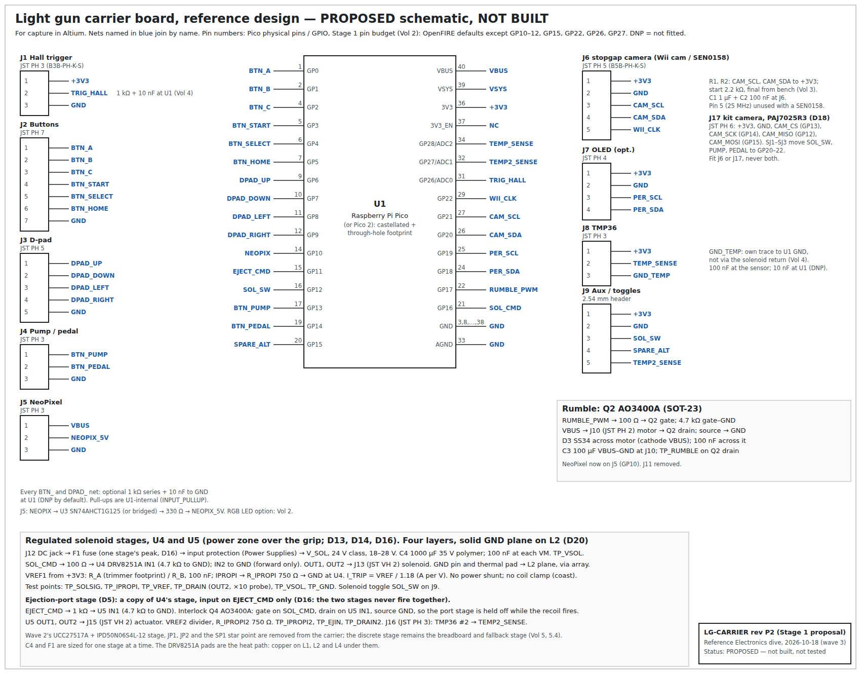
Everything on the sheet above is proposed. It collects the circuits argued in Volumes 3 to 6 into one board and gives every net a name, so that capture in Altium starts from a complete list rather than a pile of module photographs. It has not been laid out, built or tested, and several values on it are provisional until the bench measurements in Volume 7 exist. The title block says so, and any derived drawing should keep saying so until a board has passed the bring-up plan.
8.2 Stage 1: What Goes on the Carrier
The carrier holds everything except the switches, the camera, the solenoid and the actuators themselves:
- U1, the Pico (or a Pico 2, A4 stepping, which is what to buy next: decision D19, Volume 2; the footprint and pin-out are identical).
- Connectors for everything off-board (requirement R9): the Hall trigger (J1), buttons (J2), D-pad (J3), pump and pedal (J4), NeoPixel (J5), camera (J6, five-way, for the stopgap Wii camera; J17, six-way SPI, for the PixArt kit camera, decision D18), OLED (J7), the two TMP36s (J8, J16), an auxiliary header for the solenoid toggle and the spare pins (J9), the rumble motor (J10), power in (J12), the recoil solenoid (J13) and the ejection-port actuator (J15).
- The small signal parts: camera pull-up footprints and decoupling, the three camera-option solder jumpers SJ1 to SJ3 (Volume 3, 3.11), the Hall trigger’s RC filter, optional RC footprints on every button, the NeoPixel buffer footprint.
- The rumble stage (Q2) on VBUS.
- Two regulated solenoid stages (U4 and U5, DRV8251A, decision D13), sharing the input fuse and bulk capacitor, each with its own current-set divider and R_IPROPI, and the interlock Q4 that holds the port stage off while the recoil fires (decision D16; Volume 5, 5.12 and 5.13).
- Test points on every rail and every driven node (Volume 7).
How the Pico is mounted. The carrier’s footprint for U1 is the Pico’s castellated pattern with the through-holes kept, so the same board can take the Pico three ways. The choice for the first board, and why:
Table 1 — How the Pico is mounted. The carrier's footprint for U1 is the Pico's castellated pattern with the through-holes kept, so the same board can take the Pico three ways. The choice for the first board, and why
| Option | For | Against | Verdict |
|---|---|---|---|
| Low-profile sockets on the through-holes | the Pico lifts out; a dead one is swapped without rework; a Pico 2 can be tried in the same board | adds height (the socket plus the Pico’s own pins), and a socket contact is one more thing a solenoid shakes | Chosen for the bench and the first gun, with the Pico retained (a strap or printed clip) so recoil cannot walk it out |
| Soldered flat by its castellations | lowest height; the Pico datasheet describes it as “usable as a surface mount module” | replacement is rework | for the second gun, once the board is proven and the height is known to matter |
| Soldered on pin headers | robust | as tall as a socket, and no easier to replace than flat | rejected |
8.3 The Cable Leaves Through the Magazine Base Plate
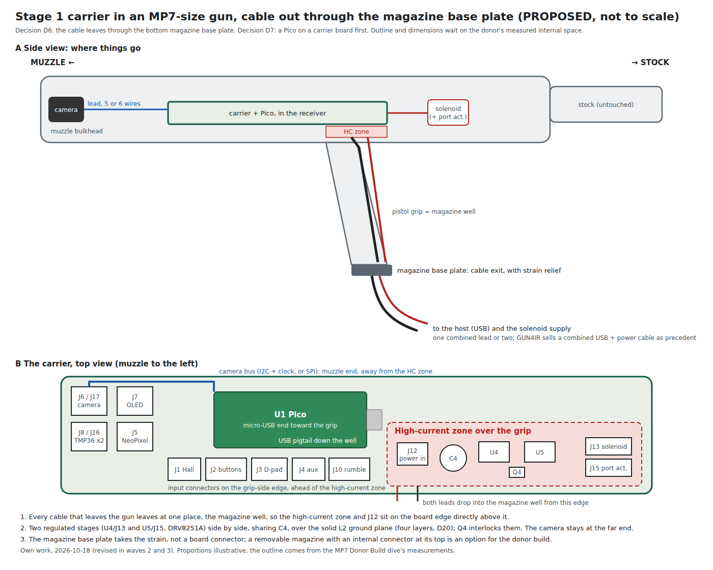
Decision (D6, 2026-10-18): for now the cable leaves through the bottom magazine base plate. It keeps the grip and the stock untouched. On an MP7 the magazine goes into the pistol grip, so the cable’s path is from the receiver, down the magazine well, and out through the base plate, which takes the strain. How the base plate is modified, and whether the magazine stays removable, belong to the MP7 Donor Build dive; the decision is revisited for the printed build.
Three things follow for the board:
- One exit, one end of the board. Both leads that leave the gun, USB to the host and the solenoid supply, leave at the same place. The power entry (J12), the bulk capacitor and both power stages therefore sit on the board edge directly above the magazine well, so the high-current wiring is as short as it can be and never crosses the board.
- USB stays on the Pico’s own connector for Stage 1. A short USB lead runs from the Pico’s micro-USB down the well to the base plate. That keeps USB data off carrier traces entirely; bringing it to a carrier connector through the Pico’s underside test pads (TP2 and TP3, Volume 2) is a Stage 2 matter. The Pico is turned on the carrier so its USB end faces the grip.
- One lead or two. The USB and the solenoid supply can leave as two cables or as one combined lead. GUN4IR sells a combined USB and power cable for its builds, which shows that a single lead through a grip is practical. A single lead puts the solenoid’s pulse current beside the USB pair for its whole length, which is the situation the OpenFIRE README’s warning about EMI disconnects describes (Volume 5); a twisted pair for the power conductors and a shielded USB pair inside the jacket are the minimum.
8.4 Sheet Organisation for Capture
The single sheet is drawn for reading. In Altium it divides naturally into five sheets joined by the net names shown:
- MCU: U1 (the Pico footprint with castellations and through-holes), local decoupling on VBUS and 3V3, the optional RC footprints on the input nets, the Hall trigger’s 1 kΩ and 10 nF.
- Connectors: J1 to J10 and J16, with the camera pull-ups and decoupling (R1, R2, C1, C2) beside J6 and the TMP36 decoupling beside J8 and J16.
- Feedback: the rumble stage (Q2) and the NeoPixel buffer footprint (U3).
- Solenoid power stage: J12, F1, the input protection positions (Power Supplies), C4, U4 with its 100 nF at VM, the VREF divider (R_A with a trimmer footprint, R_B), R_IPROPI, the 100 Ω and 4.7 kΩ on IN1, J13.
- Ejection-port power stage: U5 and the same parts, J15, and the interlock Q4 (AO3400A) with its 1 kΩ from EJECT_CMD. Drawn as a copy of sheet 4 (a repeated sheet symbol in Altium), sharing V_SOL and C4.
Wave 2 drew a star point, SP1, as a net-tie between a separate power ground and logic ground. On the four-layer board (8.9) it is dropped: the DRV8251A’s datasheet asks for its thermal pad to go to “large ground planes on multiple layers”, and a split plane under the stage would break the return path for the very edges it is meant to contain. Separation is by placement instead: the power zone’s loops close over their own part of the solid plane, and no logic return passes through it.
8.5 Net List by Block
Table 2 — 8.5 Net List by Block
| Net | U1 pin (GPIO) | Goes to | Notes |
|---|---|---|---|
| TRIG_HALL | 31 (GP26, ADC0) | J1-2 via 1 kΩ, 10 nF to GND | DRV5056A4 (fork) or DRV5023 (stock firmware), Volume 4 |
| BTN_A, BTN_B | 1, 2 (GP0, GP1) | J2-1, 2 | side buttons; optional 1 kΩ / 10 nF each |
| BTN_C | 4 (GP2) | J2-3 | the magazine-release switch |
| BTN_START, BTN_SELECT, BTN_HOME | 5, 6, 7 (GP3, GP4, GP5) | J2-4, 5, 6 | |
| DPAD_UP, DOWN, LEFT, RIGHT | 9, 10, 11, 12 (GP6 to GP9) | J3-1 to 4 | |
| NEOPIX | 14 (GP10) | U3, then 330 Ω to J5-2 | ”External NeoPixel”; J5-1 is VBUS |
| EJECT_CMD | 15 (GP11) | U5 IN1 via 1 kΩ, held low by Q4 while SOL_CMD is high | fork only (D16 interlock) |
| SOL_SW | 16 (GP12) | J9-3 via SJ1 | ”Solenoid Switch” toggle; moves to GP20 in the PixArt build |
| CAM_MISO, CAM_CS, CAM_SCK, CAM_MOSI | 16, 17, 19, 20 (GP12 to GP15) | J17-5, 3, 4, 6 | PixArt build only: SPI1 (Volume 3, 3.11); 33 Ω series footprints on CS, SCK, MOSI |
| BTN_PUMP, BTN_PEDAL | 17, 19 (GP13, GP14) | J4-1, 2 via SJ2, SJ3 | move to GP21, GP22 in the PixArt build |
| SPARE_ALT | 20 (GP15) | J9-4 | Alt Pedal, or a digital trigger; MOSI in the PixArt build, J9-4 then left open |
| SOL_CMD | 21 (GP16) | U4 IN1 via 100 Ω; Q4 gate | 4.7 kΩ to GND |
| RUMBLE_PWM | 22 (GP17) | Q2 gate via 100 Ω | 4.7 kΩ to GND |
| PER_SDA, PER_SCL | 24, 25 (GP18, GP19) | J7-4, J7-3 | I2C1, optional OLED |
| CAM_SDA, CAM_SCL | 26, 27 (GP20, GP21) | J6-4, J6-3 | I2C0; R1, R2 to +3V3 |
| WII_CLK | 29 (GP22) | J6-5 | 25 MHz for the stopgap Wii camera; unused with a SEN0158; Pedal in the PixArt build |
| TEMP2_SENSE | 32 (GP27, ADC1) | J16-2, also J9-5 | second TMP36, fork |
| TEMP_SENSE | 34 (GP28, ADC2) | J8-2 | GND_TEMP on its own trace |
| VBUS | 40 | Q2 motor supply, J5-1, C3 | 5 V from USB |
| +3V3 | 36 | J1, J6, J7, J8, J9, J16, J17, both VREF dividers | under 300 mA in total; the Hall sensor draws up to 10 mA |
| V_SOL | — | J12, F1, C4, U4 and U5 VM | the power stages only; 24 V class, 18 to 28 V (D14) |
| VREF1, VREF2 | — | U4, U5 VREF | set point: I_TRIP = VREF / 1.18 A per volt with R_IPROPI 750 Ω |
| GND | 3, 8, 13, 18, 23, 28, 33 (AGND), 38 | everywhere, one solid plane on L2 | the power zone’s returns stay in the power zone by placement |
The pin numbers are the Pico’s physical pins with the Stage 1 assignment of Volume 2. With stock firmware the app must be told about the moved functions (Trigger on GP26, External NeoPixel on GP10, Solenoid Switch on GP12, Wii Cam Clock on GP22); EJECT_CMD and TEMP2_SENSE do nothing until the fork reads them, and the PixArt build needs a firmware that reads the PAJ7025 (Volume 3, 3.11). Any pin can still be moved, subject to the I2C pairing rule for the camera.
8.6 Decisions Carried Into the Schematic
Table 3 — 8.6 Decisions Carried Into the Schematic
| Decision | Value on the sheet | Argued in |
|---|---|---|
| MCU | Pico on a carrier, Pico 2 compatible (D2, D7); buy Pico 2 A4 and one ESP32-S3-DevKitC-1 (D19, D25) | Volume 2 |
| Pico mounting | castellated + through-hole footprint, socketed for Stage 1 | 8.2 |
| Pin assignment | Stage 1 pin budget | Volume 2 |
| Trigger | Hall-effect on GP26: DRV5056A4 (fork) or DRV5023 (stock) (D8) | Volume 4 |
| Camera | J6 five-way for the stopgap Wii camera; J17 six-way SPI for the PixArt PAJ7025R3 kit camera; SJ1 to SJ3 select the build (D18) | Volume 3 |
| Gate and rumble pull-downs | 4.7 kΩ | Volume 2 (erratum RP2350-E9), Volume 5 |
| Camera pull-ups | footprints, about 2.2 kΩ total to start | Volume 3 |
| Input filtering | footprints only | Volume 4 |
| TMP36 ground | dedicated return, both sensors | Volume 4 |
| Solenoid drive | regulated current, DRV8251A per stage, set by VREF (D13) | Volume 5, 5.12 |
| Recoil rail | 24 V class, 18 to 28 V; the discrete stage’s 12 V Zener feed, no JP1 (D14) | Volume 5 |
| Ejection-port drive | identical second regulated stage on EJECT_CMD only; Q4 interlock (D5, D16) | Volume 5, 5.13 |
| Clamps | none on the regulated stages: the bridge coasts the coil’s energy back to C4; input TVS per Power Supplies | Volume 5 |
| Power connectors | JST VH (10 A per LCSC’s listing) | Volumes 4 and 5 |
| Status light | one NeoPixel with a buffer footprint | Volumes 2 and 5 |
| Bulk capacitance | 1000 µF 35 V polymer plus 100 nF at each VM | Volume 5 |
| Current sense | IPROPI through 750 Ω to a test point, per stage; no power shunt | Volumes 5 and 7 |
| Fuse | F1, value from one stage’s measured peak (the stages never fire together, D16) | Volume 5; Power Supplies |
| Layers | four (D20) | 8.9 |
| Cable exit | magazine base plate (D6) | 8.3 |
The fuse is the one item the sheet leaves unvalued. Its rating depends on the peak current of one stage (D16) and on the adapter, measurements not yet made, and its type (a slow-blow cartridge or a PTC) is a power-supply decision for the Power Supplies dive. Reverse-polarity protection at J12 belongs to the same discussion; the sheet reserves the position.
8.7 The Floorplan
The arrangement follows from three facts. The camera has to be at the muzzle. Every cable that leaves the gun leaves through the magazine well (8.3). And the high-current loops should be as far as possible from the camera bus and its clock. That puts the power stages on the board edge above the grip, beside the cable entry, and the camera connector at the other end.
The solenoid itself sits wherever the mechanical design puts it, which in an MP7 conversion is likely in the receiver above or behind the grip. Its two leads, twisted, run from J13 to the coil, and the port actuator’s from J15; neither should run alongside the camera lead.
One consequence of the Pico’s pin-out is that SOL_CMD (pin 21) leaves the Pico at the corner nearest the camera pins, while the power stages are at the grip edge. That trace crosses part of the board. It is a logic signal, so this is harmless provided it runs over unbroken ground and enters the power zone beside C4, over the solid L2 plane. The same applies to EJECT_CMD from pin 15.
8.8 Layout Rules
- The pulse loops. For each stage, C4 → U4’s VM (with its 100 nF at the pin) → OUT1 → J13 → coil → OUT2 → U4’s pad → the L2 plane directly beneath → back to C4, entirely within the power zone over the grip, as small in area as the parts allow. The two stages sit side by side, not one inside the other, and C4 and J12 sit between them.
- The ground. One solid plane on L2 (8.9), under the whole board and unbroken under the power stages (D20). Each DRV8251A’s thermal pad goes to it through a via array, as TI’s datasheet asks. No logic return is routed through the power zone, and no power return is routed through the logic zone: separation by placement, not by a split.
- The camera bus and clock. CAM_SDA, CAM_SCL and WII_CLK from U1 pins 26, 27 and 29 to J6, and the four SPI nets from pins 16, 17, 19 and 20 to J17, run over continuous ground, as short as the floorplan allows, and never enter the high-current zone. R1 and R2 sit at the U1 end; C1 and C2 at J6. WII_CLK and CAM_SCK are routed with a ground on each side. SJ1 to SJ3 sit beside U1 so that the unused branch of each is a stub of a few millimetres.
- The TMP36 returns. GND_TEMP for each sensor runs as its own trace to a U1 ground pin, not through the power zone.
- The Hall trigger. TRIG_HALL’s 10 nF sits at U1’s pin 31 with its ground to AGND (pin 33); the trace stays away from the gate-drive and clock nets.
- The set point and the mirror. Each stage’s VREF divider and R_IPROPI return to the plane beside that driver’s GND pin, not across the board, so that the mirror voltage is measured against the driver’s own ground. VREF is decoupled at the pin.
- Heat. Each DRV8251A dissipates about 2.8 W while driving 2.5 A and about 0.45 W averaged over autofire (Volume 5); its pad, the via array and copper on L1, L2 and L4 under it are the heat sink.
- Test points. On the top side, reachable with the shell half open, each with a ground pad beside it (requirement R10, Volume 7). TP_DRAIN (each stage’s OUT2) is spaced for a ×10 probe tip and ground spring.
- Mechanics. Mounting holes at both ends and outside the power zone. C4 is the heaviest part and the power connectors the most handled; all see the recoil, so all are anchored (adhesive under C4 if it is a tall can; through-hole or reinforced pads for J12, J13 and J15). The socketed Pico is strapped.
- USB. On the Stage 1 board the Pico’s own micro-USB is used and the lead runs down the magazine well (8.3).
- Copper weight. The high-current traces carry one stage’s peak current at a time (D16); they are sized for it and for the pulse heating of a few tens of milliseconds, with the board house’s current-capacity calculator once the peak current is known.
8.9 Stack-Up and Fabrication
Decision (D20, 2026-10-18): four layers for the first carrier, for a solid ground plane under the solenoid stage. The proposed stack-up:
Table 4 — Decision (D20, 2026-10-18): four layers for the first carrier, for a solid ground plane under the solenoid stage. The proposed stack-up
| Layer | Use |
|---|---|
| L1, top | components; signals; short power pours in the power zone (V_SOL to each VM, OUT1 and OUT2 to J13 and J15) |
| L2 | solid ground, unbroken across the board; the reference for every L1 signal and the return for the pulse loops |
| L3 | power: a V_SOL pour under the power zone only; 3V3 and VBUS pours under the logic zone, kept apart from V_SOL |
| L4, bottom | the few signals that will not fit on L1; ground fill stitched to L2, with extra copper under the drivers’ pads |
Why each choice, and why not the alternatives:
- Ground on L2, next to the components, because the loops that matter (the pulse loops, the camera bus, the 25 MHz clock, the SPI clock) are on L1, and a plane one dielectric away gives each the smallest loop. Ground on L3 would put the power plane between the signals and their return.
- No split plane. Wave 2’s two-layer thinking joined a separate power ground to logic ground at one star point. On four layers that is the wrong tool: the DRV8251A’s pad wants the plane, a slot under the stage forces the edges’ return currents around it, and the separation it was meant to give comes as well from placing the power zone at the grip end with nothing else in it.
- V_SOL on L3 under the power zone only, so the 24 V-class rail is never under the camera bus or the clock.
- Two layers would work, as wave 2 said, with the bottom layer almost all ground. It was the fallback; the cost difference at prototype quantities is small, and D20 settles it.
A standard 1.6 mm four-layer build from a prototype board house, with 1 oz outer copper, is the starting point; the exact dielectric thicknesses are the house’s standard stack, chosen in Altium’s layer stack manager, because nothing on this board is impedance-controlled except USB, which stays on the Pico’s own connector in Stage 1. The lab’s reflow oven and rework station handle the SOT-23, HSOP-8 (with its exposed pad, which wants stencil paste and reflow rather than an iron) and TO-252 parts, and the Pico’s castellations if it is ever soldered down.
8.10 Stage 2: the Custom Board, Later
These are notes to keep, not a design. Stage 2 starts when Stage 1 has passed the bring-up plan in a real gun.
- The microcontroller goes onto the board. A bare RP2040, or an RP2350 if the analog trigger’s ADC or the fork’s needs argue for it (Volume 2), with QSPI flash, a 12 MHz crystal, a regulator and USB laid out to Raspberry Pi’s hardware design guide. The firmware then sees a “generic” board, mapped by hand in the app or given its own preset in the fork. If the pin budget has overflowed by then, the RP2350B’s 48 GPIO and 8 ADC inputs are the obvious step.
- USB-C where the cable leaves. With the chip on the board, the USB connector can sit wherever the cable exit is, for a printed build perhaps no longer the magazine base plate.
- Its shape comes from the gun. The outline follows the measured donor, or the printed shell, rather than the Pico’s rectangle.
- What Stage 1 must hand over: the measured peak current of each stage and the fuse value; the current set points; whether the DRV8251A’s chop is audible; the camera pull-up values; whether the Wii camera runs from its own oscillator (and so whether WII_CLK survives); the Hall sensor version and magnet; the rumble motor’s current; and every change made to the carrier during bring-up.
- The wireless path (requirement R12) is a different board again: an ESP32-S3, a battery and its charger, and the PixArt kit camera, which that port already reads. Whether the kit’s board is this one depends on the D25 dongle trial (Volume 2). That belongs to the Power and Connectivity dives.
8.11 What Must Be Known Before Layout Freezes
Table 5 — 8.11 What Must Be Known Before Layout Freezes
| Input | Source | Blocks |
|---|---|---|
| Gun’s internal envelope: receiver length, width, height, mounting points | For the first gun, the 3D-printed MP7: the printed shell sets the board’s maximum outline and carries its mounting slots or posts (decision D44; MP7 Printed Build, Volume 5). For a later airsoft donor: MP7 Donor Build measurements | board outline, C4 height, socket height, connector orientation |
| Magazine well and base plate: free cross-section, path from the receiver | MP7 Donor Build | the cable’s diameter, one lead or two, J12’s position |
| Solenoid and port-actuator peak currents and inductance | Volume 7, stage 4 | F1, J13 and J15 ratings, trace widths, the VREF set points |
| Camera lead capacitance; Wii camera clock arrangement | Volume 7, stage 1 | R1, R2; whether WII_CLK needs routing care |
| Chop frequency and audibility of the DRV8251A | Volume 7, stage 4 | whether the regulated stage stays or the discrete chopper replaces it |
| Which camera build the first board carries | Volume 3, 3.11; the firmware route | SJ1 to SJ3, J6 or J17 fitted |
| Rumble motor current | Volume 7, stage 3 | whether the motor stays on VBUS |
| Camera body size and thread | Volume 3 | the muzzle bulkhead, not the board, but it fixes J6’s position |
Sources
- TeamOpenFIRE, OpenFIRE-Firmware v6.2,
BOARDS.md, and OpenFIRE-BoardsOpenFIREshared.hat commit a019e91 (read 2026-10-18). - Raspberry Pi Ltd, Raspberry Pi Pico Datasheet: castellated-module use, test pads, power (read 2026-10-18).
- GUN4IR, store listing (combined USB and power cable), https://gun4ir.com/collections/all (read 2026-10-18).
- The component datasheets cited in Volumes 3 to 6 of this dive.
- LCSC product listings for the JST connectors (read 2026-10-18).
- Texas Instruments, DRV8251A datasheet, SLVSFU6, January 2022: pin functions (thermal pad) and layout guidelines (read 2026-10-18).
- PixArt Imaging, PAJ7025R3 Product Datasheet, version 1.0, reference circuit (as cited in Volume 3).
Comments (0)